I recently started lessons to get my private pilot license and realized a watch would be really helpful. Naturally my response was to build one from scratch rather than buy one. I've really hopped on the LED train with my LED visualizer projects, so the watch had to use LEDs instead of other display types. While I would love to design a mechanical watch, I just don't have the resources to make any of the parts - so digital was the only option. LEDs are much more vibrant than something like an LCD display.

CAD mockup of my first idea for the watch design. The face is made of 60 blue LEDs, and can only display hours and minutes.
I started by sketching out different concepts for the watch. Any design needed to be waterproof, so I eliminated any physical buttons from the concepts. I also needed to be able to purchase or make any of the components. My first though was to make a digital watch display with a set of the smallest SMD LEDs I could find on digikey. This led me to come up with a grid of LEDs (5 x 7) for each digit (4 digits: hours and minutes). I wasn't really feeling the design, and decided a mix with a classic analog design would be the best. At the same time I ran across two components that led to my final design. The first was an LED Driver chip, the IS31FL3733. This chip is an I2C LED matrix driver, capable of driving a grid of 16 by 12 (192!) LEDs. The other component was a 1mm square RGB LED. These LED chips have a red, green, and blue LED connected by a common anode. An analog watch face with 60 of these LED chips (one for each minute/second) requires a driver for 180 LEDs. The combination of these LEDs and the driver chip made for a simple control of the watch face.
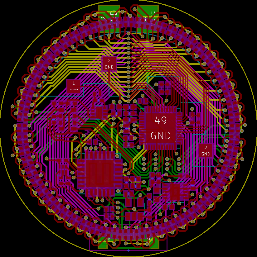
PCB layout for the watch. Traces fan out from the LED driver chip, leaving little room for other components.
This was my first custom PCB in a while aside from some PCBs I've made for various projects in grad-school. I decided to use KICAD for my schematic and layout program. It's open-source and seemed to have any feature I would need to design the PCB. I figured the PCB would need to be four layers, so this was the best option without having to pay for a license. KICAD was very intuitive for me, and I was able to start designing after doing a simple tutorial. The layout for this project was very time consuming. The 60 watch face LED chips are electrically arranged in a grid, but they're not mounted in a grid. This really forced me into the four layer PCB. The face is broken into four quadrants of 15 LED chips. Each quadrant gets its own R, G, and B cathode control lines, while four LED chips (one per quadrant) share each anode control line. This forms a grid of 15 x 12, which is slightly less than the available outputs for the LED driver chip. A major difficulty in laying out the board was finding areas to place vias between the board layers. The cathode control lines cover nearly the entire PCB, while the anode control line vias form a wall around the perimeter of the board.
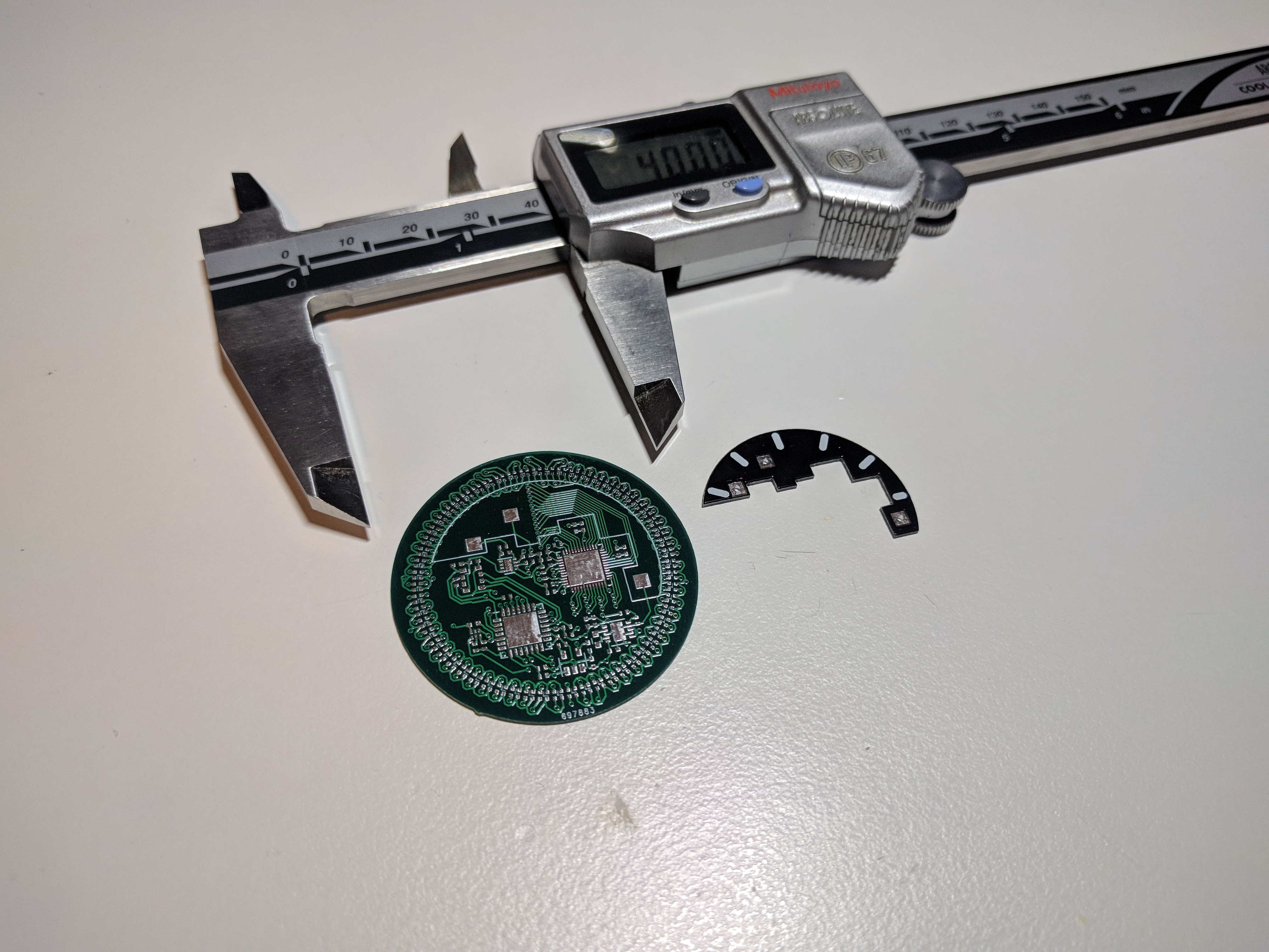
Watch and capacitive button PCBs. The capacitive button PCB is soldered to the main watch to help isolate the button from the LED power lines.
I ordered the PCBs from SeeedStudios Fusion PCB service. I had a number of friends order boards from them with great results, so I figured it was worth a try. The price was really good, and the turnaround was reasonable (~2 weeks). I was also able to order a matching solder paste stencil to make assembling the surface-mount parts easier. This was my first project with small SMD components as well as my first time using solder paste.
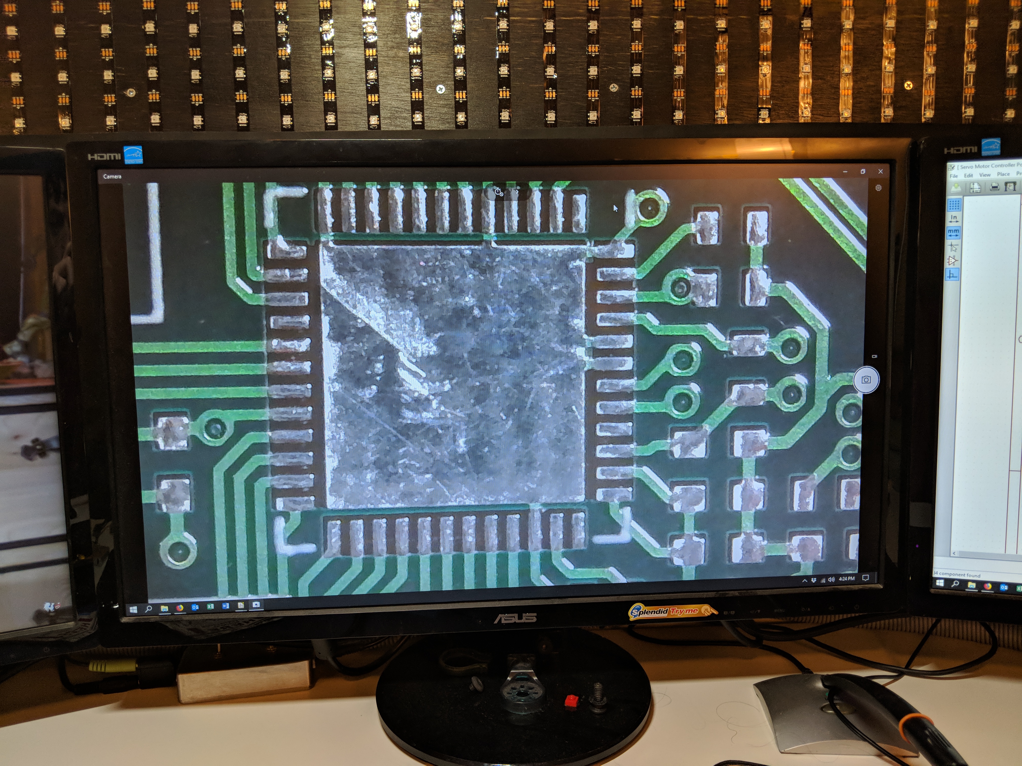
USB microscope view of the QFN footprint for the LED drive chip. This microscope was essential to solder the tiny SMD components.
Placing the components was quite a challenge. I was forced to use 0402 passive components to get all the necessary components to fit in the layout. A good set of needle (actually sharp) tweezers makes a big difference when trying to move components around. Squeezing a component too tightly often led to launching a resistor across the room. Overall I only dropped about two components out of the ~100 required to complete the watch. I used a SMD rework heatgun to melt the paste and solder the components down. I was careful to not apply too much heat and possibly burn or melt one the components. Some components like the clock chip are more sensitive to heat due to the resonators used inside. It is also important to check the humidity requirements for the components. Many of the components I used had humidity limits before soldering. From what I understand, if a component is exposed to high humidity it can absorb water. This water will then boil while soldering and damage the component. If you live in a high-humidity environment, then you need to pay attention to these warnings and use proper dehumidifying bakes before soldering.
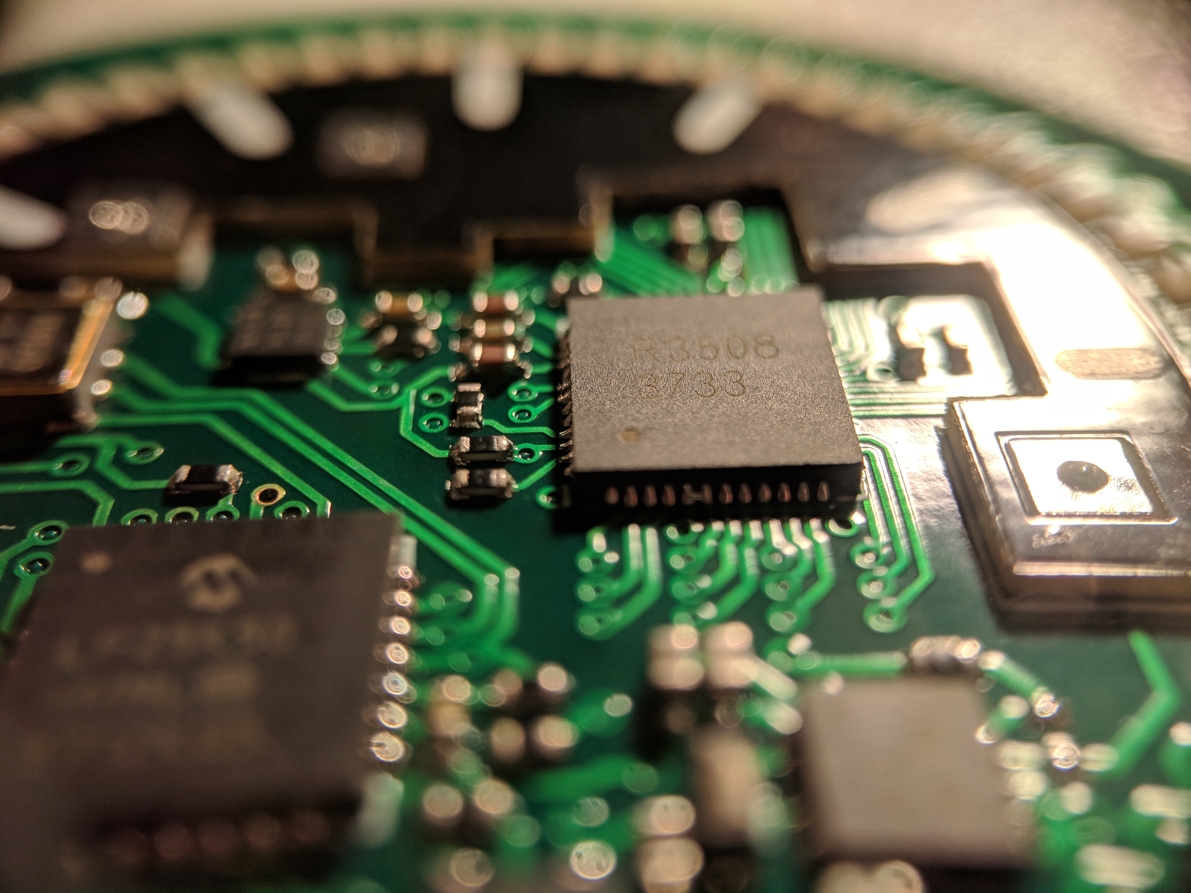
Soldered watch PCB. A single set of pins was bridged on the LED driver chip.
Some minor rework was required to complete the watch. A few pads on the QFN packages were shorted. A careful swipe with a knife while heating the chip was enough to split the two pads. I was surprised by how few of the QFN pads were bridged after soldering. The surface tension of the solder really wants to keep each pad separate. I think the pads that did short were caused by me sliding the chip laterally when placing it with tweezers. I may try to build a manual pick and place machine if I have to place a large number of these high pin density packages in the future.
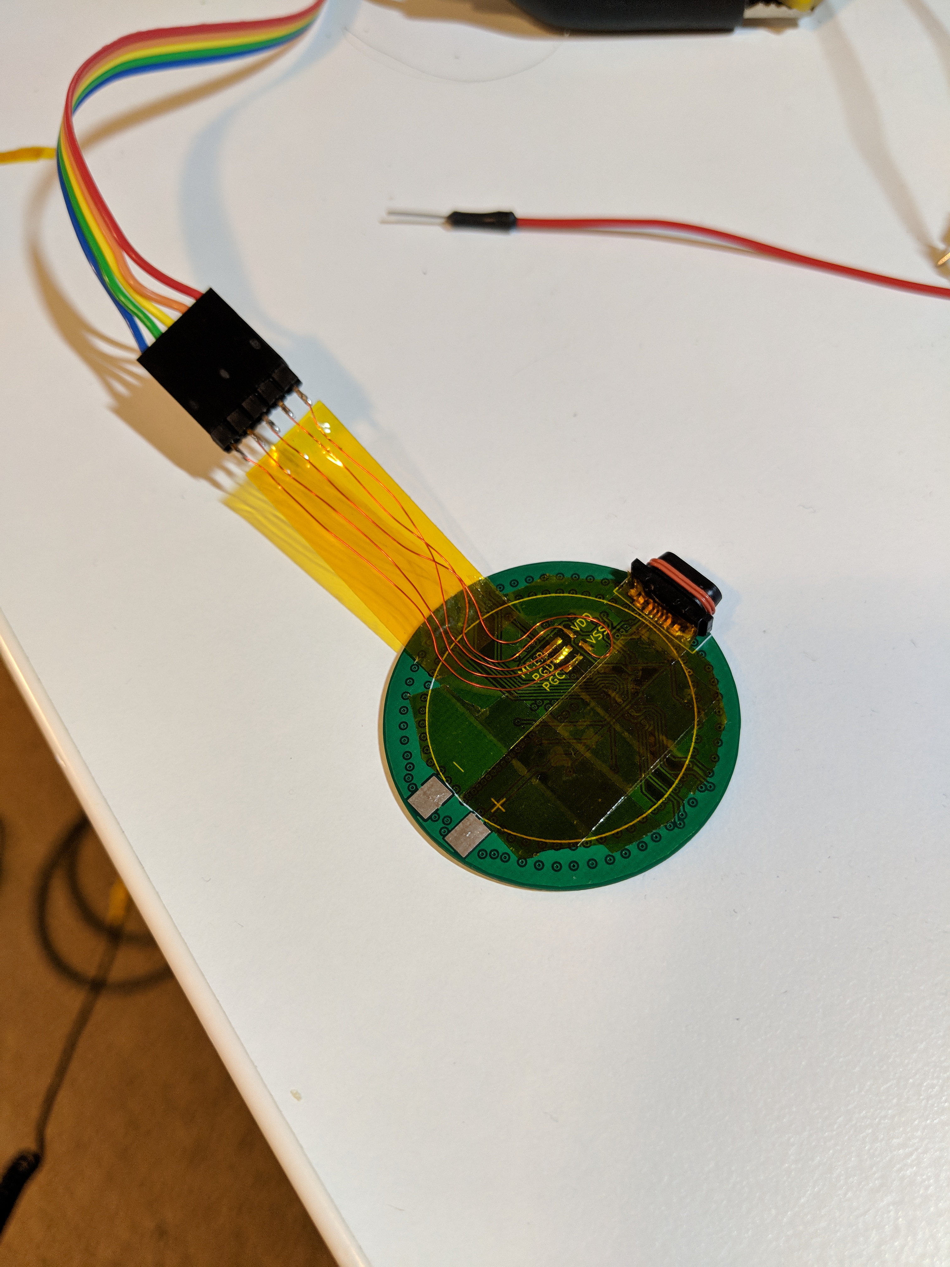
Complete PCB with programming pins. A home-made flat flex cable was used to keep the connections thin enough for the battery to be soldered on top and still lay flat with the watch PCB.
The watch has to be programmed initially using the PICkit3 (a programmer/debugger for microprocessors by Microchip). Due to packaging limitations I had to place these programming pads underneath the battery location, which is very inconvenient due to the battery being soldered down to the PCB. My original intent was to program the watch once and then use a bootloader to program it over the USB port. Unfortunately at this time I haven't written or found a bootloader for this microprocessor, so any program must be uploaded by the programming port. A partial workaround was a home-made flat flex cable that breaks out the programming pads. I used kapton tape and thin enameled magnet wire to form the traces. This can be folded over the battery for the final assembly of the watch. The code for the watch was pretty simple due to the two main functions (LED driving and time keeping) being handled by a set of I2C chips. I used an I2C temperature compensated real time clock. With one command I can have it send the hours, minutes, and seconds back to the microprocessor. The LED driver chip is also a simple set of write commands to drive the LEDs. The microprocessor handles the USB serial emulation. I did not currently write the USB emulation myself, as microchip has many helpful libraries and code examples to handle things like USB serial port emulation. Eventually I plan to write the USB code myself as an education project, but for now I just wanted to get a functional watch as quickly as possible.
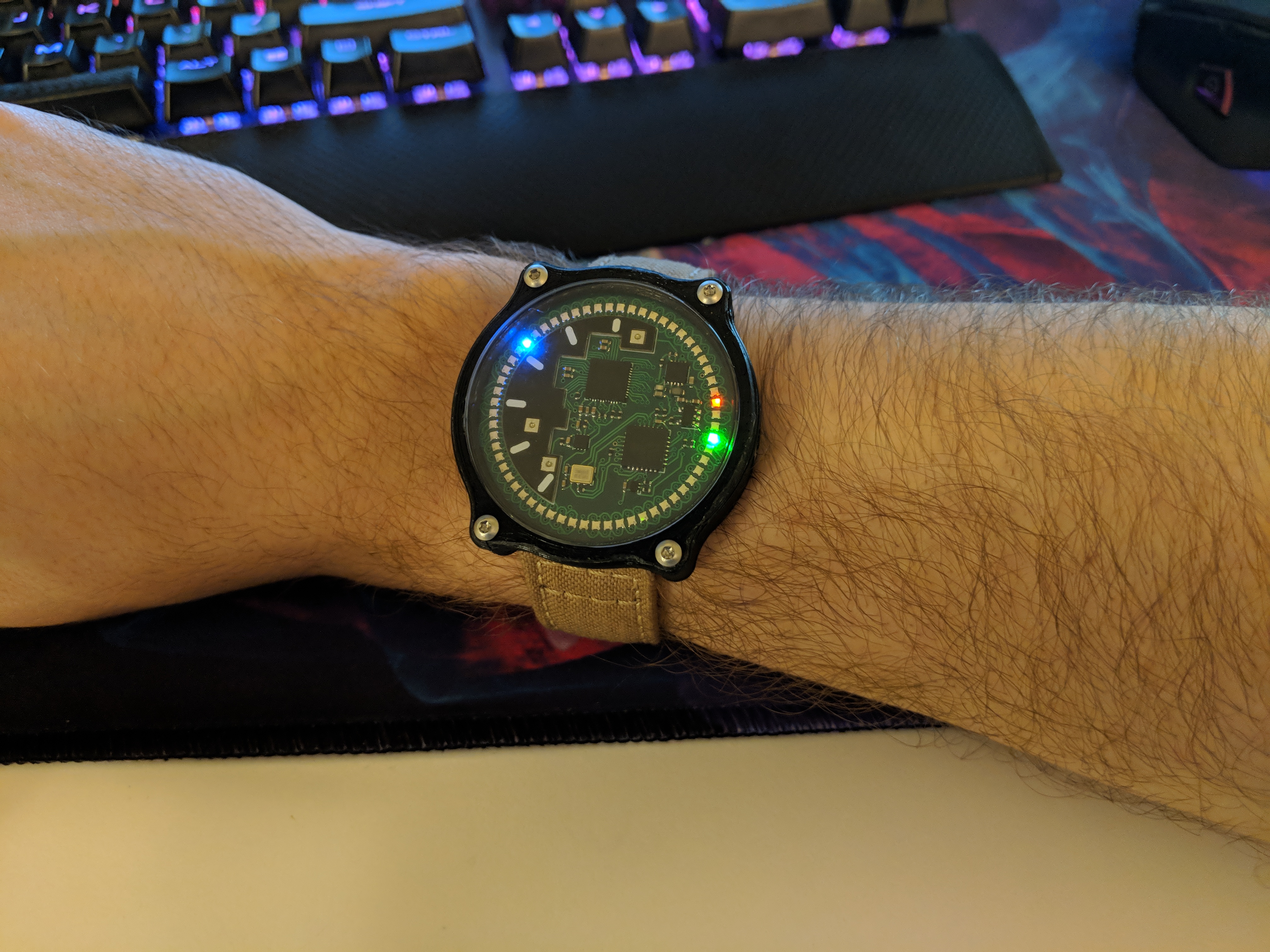
The completed watch telling time(10:16:13). Blue: hours, Green: minutes, Red: seconds.
As always the watch is still a work in progress. The case is currently 3D printed because I haven't had the free time or machine time available to mill the case from stainless steel. The code is in what I call a "MVP" state, meaning minimum viable product. My goal was to make an LED watch, and telling time is the only feature currently available on the watch. Time is set through the USB serial port. I made a small script in python that automatically pulls the time from my computer and loads it into the watch through the time setting serial menu. I tested the capacitive button, but found it to be not sensitive enough to sense finger through the glass. I realize this was a mistake I made in the button PCB design. My breakout board for the capacitive button included a ground plane to shield from the LED power lines. Looking back at the datasheet, it clearly said to not use a ground plane on the button. The ground plane dramatically increases the capacitance of the button, preventing the chip from sensing the capacitance change caused by my finger approaching the button. Eventually I will make an upgraded form of the watch and correct this issue.